DESCRIPTION

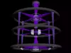
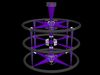
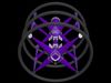
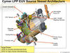
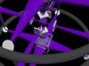
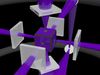
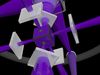
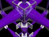
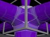
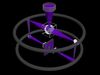
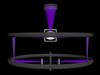
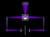
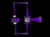
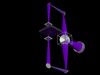
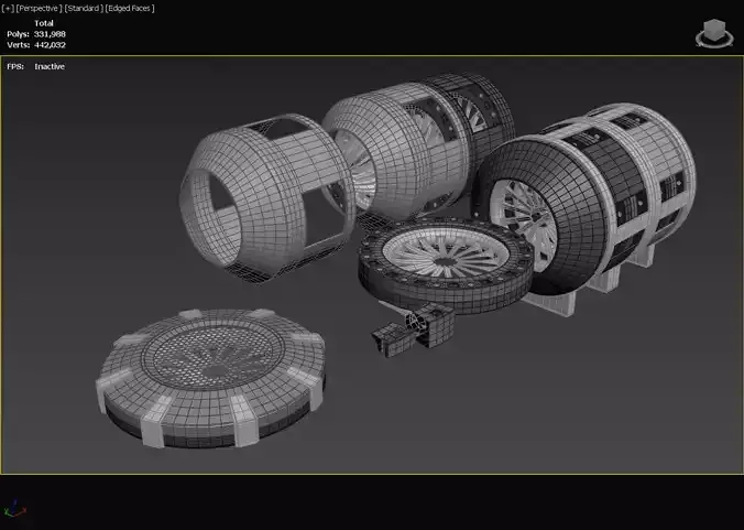
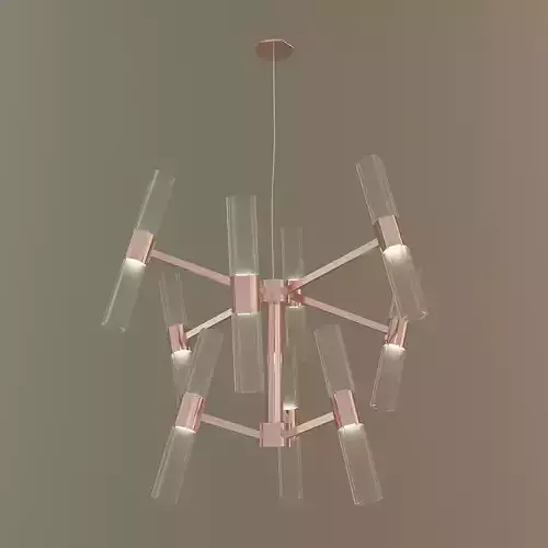
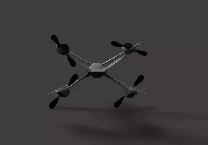
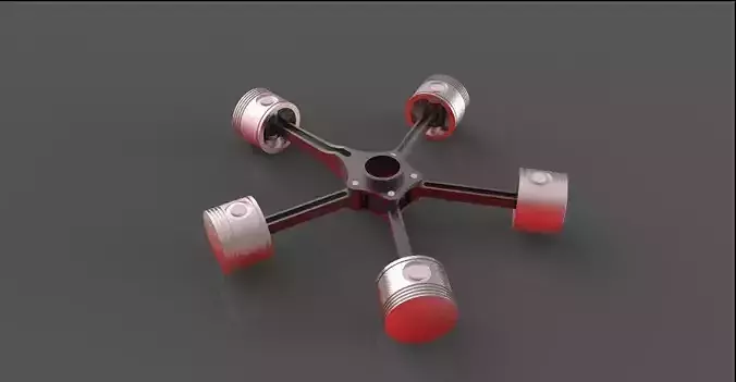
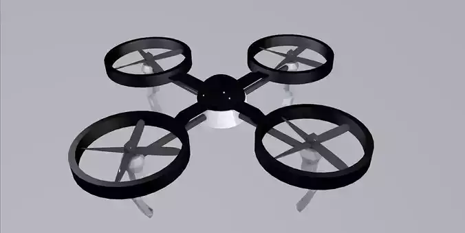
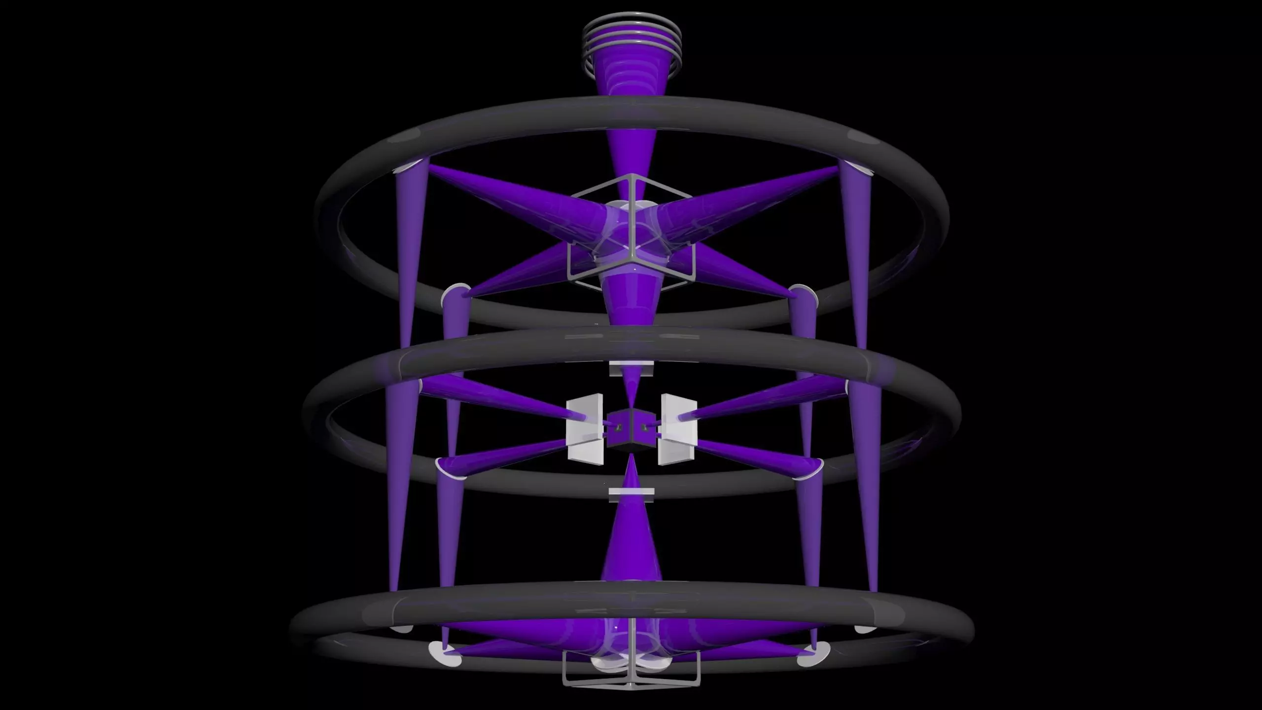
6D Dutch Semi-Conductor Wafer Method - 1 Laser signal splits into 6x ALL Fields EUV Surfaces - Concept.

1 Laser can be split into 6 directions, recmobining to 6 or more surfaces, to work on at thsame time, for perhaps the same chip, but atleast we can split the EUV in two parts, finally working on two sides of the same chip at once, using one laser boost,to create two surfaces. the more surfaces we can create semi-conduictors on, the more energy we save, and more chipswe produce in the same time. a final cubic 6D semiconductor could be placed in a final cylindrical die again, insidea conductive material once more, to be able to reach all sides of the 6D semi-conductor cube. if one laser shone downward,and an angled round mirror was beneath it, that could turn 360 degrees, you could project euv in a radial sequence, working on chips all in a 360 degree circle, one after the other or again with a split into 4 or 6 signals optical euv laser.the same 10kw blast can be used multiple times, split into multiple signals, working on multiple surfaces. perhaps in the future even a dodecahedron semi-conductor lol. lets work on two or more sides of the same coin.or split 3 lasers into 2 signals for 6 surfaces with 1x usable motion all 6x mirrored masks. or simply turn over a single waver cylinder to work on the backside quickly and without much recalibration.

the future is now.

thank you for reading, thank you for your support. please like and subscribe for more cool recipes.

i live off of comments and your likes, please, if you enjoyed, help me out, drop a like.

Thanks for being here, and remember to be kind today.
REVIEWS & COMMENTS

See what other buyers think about this model - real feedback on quality,
accuracy, and usability.
View all
0
0
2
Raqia-Design
Raqia-DesignSeller of this model
This user is the seller of this model
they should use TWO SIDES of the same chip, making the layers of semi conductors on BOTH sides of the wafer, from a single split EUV laser beam, at the same time..... one energy burst, 2 chip sides.... double the amount of transistors on the same substrate... a mirror image.....
Raqia-Design
Raqia-DesignSeller of this model
This user is the seller of this model
Thank you for reading, thank you for your support. please like and subscribe for more cool recipes. i live off of comments and your likes, please, if you enjoyed, help me out, drop a like. My Models: https://www.cgtrader.com/raqia-design My Models https://www.artstation.com/dennis-the-menace My video's: https://www.youtube.com/channel/UCGtt... Tips: https://paypal.me/dennisarends01 Thanks for being here.

6D Dutch Semi-Conductor Wafer Method - Concept 3D model

$7.00
Editorial License (no AI)
Hire
Like this model to show appreciation to the designer.
See how many times this model was viewed.
Share this model to support the designer and boost their visibility.
File formats
STL
Stereolithography<br />File Size: 7.08 MB
OBJ
OBJ | 2 files<br />File Size: 8.44 MB
FBX
Autodesk FBX<br />File Size: 791 KB
MAX
Autodesk 3ds Max<br />File Size: 2.46 MB
OTHER
Other<br />File Size: 15.5 KB
Provided by designer
Information and details shared directly by the model's designer.
3D Features
Materials
The model has material settings that define how surfaces look (color, shine, transparency, etc.).
3D printing
Indicates whether the designer marked this model as suitable for 3D printing.
Model is not 3D printable
The designer indicates this model is intended for digital use only (rendering, animation, or AR/VR) and not for 3D printing.
Unwrapped UVs
Publish date
Model ID
Chat